


The Amplifiers are suitable for frequency bands ranging from 20MHz to 6GHz,the output power can be customized from 1 Watts to 200 Watts. The amplifiers utilize the cutting edge Solid-State technologies, such as GaN, LDMOS, with multi-measures, such as advanced broadband RF matching networks and combining technologies(Doherty design),then provide exceptional performance with high gain, high efficiency, wide dynamic range, low distortions, and good linearity. The amplifiers have a variety of applications including Aerospace, Military, Radar, Electronic Warfare, Communication system(Repeater/BDA,RF Jammer, IMSI catcher), SATCOM, EMI/RFI testing, Lab test and measurement, PIM testing and so on. Action Technologies’ ISO9001:2015 quality management system assures consistent performance, high reliability and ruggedness.
High gain and high efficiency
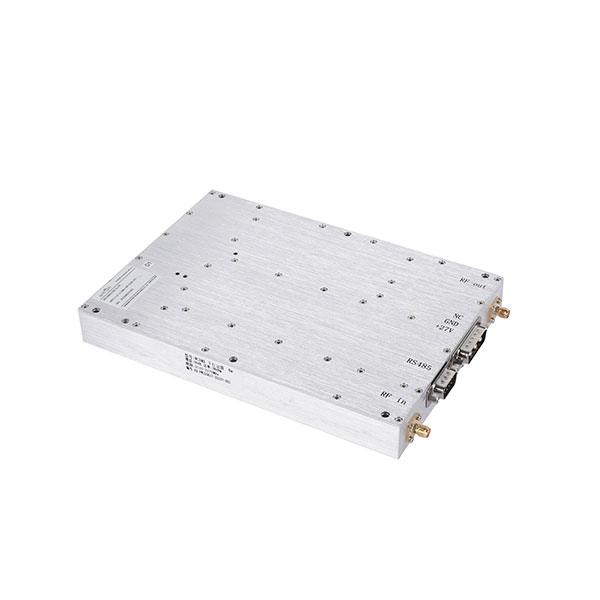
High input/output isolation
Ultra-wide band
Compact design and lightweight
Built-in protection and monitoring circuits
| Items | Specifications | |
| Downlink/Tx | Uplink/Rx | |
| Frequency Range | 450~1500MHz | 450~1500MHz |
| Max Output Power | 2*10W | -- |
| Gain@25℃ | 40±2dB | 10±2dB |
| Passband Ripple | ≤2.5dB(Only Valid Frequency Bands are Required: the U Band 450-650MH and L Band 1000-1500MHz Must Meet the Requirements, and U and L do not Work Simultaneously) | |
| ACPR@20MHz LTE | ≤-30dBc(Effective Frequency Band) | -- |
| PAR=8dB at 0.01 | ||
| EVM | ≤5%(Effective Frequency Band) | -- |
| Isolation of Sending and Receiving | ≥55dB | |
| Switching Time for Sending and Receiving | ≤6us | |
| Noise Figure | -- | ≤3.5dB |
| Input VSWR | ≤1.5 | ≤1.5 |
| Output VSWR | Not Required | ≤1.5 |
| Maximum Input Anti Burn Power | 15dBm(Not Damaged) | 10dBm(Not Damaged) |
| Power Amplifier Output Protection | The Power Amplifier Remains Undamaged After 10 Minutes of Open Circuit Operation | - |
| Working Voltage | 9-30V |
| Working Current | ≤2.5A@12V |
| Monitoring Function | Not Have |
| Working Temperature | -40℃~+80℃ |
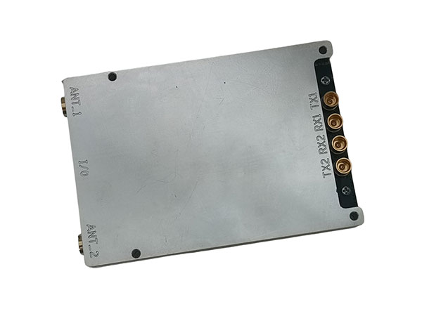
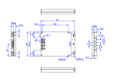
| Dimension | 75*54*10.5mm |
| Interface Definition | Model Power Supply and Control Connector: |
| PIN1:VCC@Supports 9-30V; | |
| PIN2:VCC@Supports 9-30V; | |
| PIN3:GND@Grounds; | |
| PIN4:GND@Grounds; | |
| PIN5:PAEN1@Channel 1PA Control Signal, High Level Effective (3.3V), Maximum Output Current 5MA; | |
| PIN6:LNAEN1@Channel 1LNA Control Signal, High Level Effective (3.3V)Effective, Maximum Output Current 5MA; | |
| PIN7:PAEN2@Channel 2PA Control Signal, High Level Effective (3.3V), Maximum Output Current 5MA; | |
| PIN8:LNAEN2@Channel 2LNA Control Signal, High Level Effective (3.3V)Effective, Maximum Output Current 5MA; | |
| RF Connector Interface Definition | TX1: - @Channel 1 Baseband Signal Output; |
| RX1: - @Channel 1 Baseband Signal Input; | |
| TX2: - @Channel 2 Baseband Signal Output; | |
| RX2: - @Channel 2 Baseband Signal Input; | |
| ANT1: MCX SMT Mother Seat@Antenna Port1; | |
| ANT2: MCX SMT Mother Seat@Antenna Port2; |
TDD-LTE2300 RF Power Amplifier Modules For Repeater / IMSI Catcher
20W 43dBm LTE2100 RF Power Amplifier Module For Repeater / IMSI Catcher
LTE2600 RF Power Amplifier Modules For Repeater / IMSI Catcher
20W 43dBm LTE2600 RF Power Amplifier Modules For Repeater / IMSI Catcher
490MHz RF Power Amplifier Module For Repeater / IMSI Catcher


With years of rich on-site experience, our products, including cellular repeater, TETRA BDA, DAS, BTS/IBS components as well as NMS software system have been deployed in over 30 countries around the world.


 Phone: +86-755-86238970
 Fax: +86-755-26495994
 Skype: action.technologies
 Add: 3/F, Lifeng Building, 42# of Liuxian 1st Road, Bao'an 71st District, Shenzhen 518101, China


